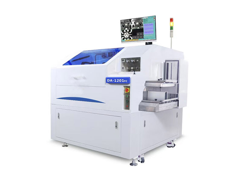
| Projects | DA1201FC | |
|
Crystal overlay mode/ high-precision solid crystal mode |
XY placement accuracy | ±10-15μm @3σ |
| Chip rotation |
5mm≤Chip size≤10mm ±0.15°@ 3σ;
1mm≤Chip size≤5mm ±0.3°@ 3σ; |
|
| Solid crystal mode | XY placement accuracy | ±10-25μm @3σ |
| Chip rotation |
Chip size≥1mm ±0.5°@ 3σ; Chip size≤1mm ±1°@ 3σ |
|
| material handling capability | Microchip |
0.25x0.25mm-9x9mm( Standard) 0.15x15mm-15x15mm(Optional) |
| Chip thickness |
0.076-1 mm(3-40 mils, Standard) the thinnest to0.05 mm (2 mils,Optional) |
|
| Fuse |
long:100-300mm ;wide:30-100mm; 0.1-0.8mm(Standard)0.8-2.0mm(Optional) |
|
| Box size |
110-310mm x20-110mm x70-153mm (Length x Width x Height) |
|
| Wafer workbench | Wafer size | Maximum 12 "Wafer size |
| Automatic theta calibration | ± 10 ° range | |
| Maximum wafer angle correction | 360° | |
| Keyhead system | Bonding strength | 20-500 g(programmable) |
| Clamping systems | Track width standard | 30- 100 mm(customizable) |
| Image recognition system | PR system | 256 gray levels |
| resolution (of a photo) | 1920 pixelx2560 pixel (customizable) | |
| PR accuracy | 5M(1920x2560 pixel) FOV (16mm;x1,x2,x4) | |
| Angular Tolerance | ±0.1° | |
| Machine size and weight | Size |
2350×1570x1900 mm (Length x Width x Height) |
| Weight | 1800kg |